- Sorry, this product cannot be purchased.
Product Details
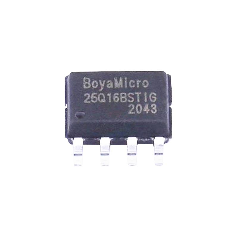
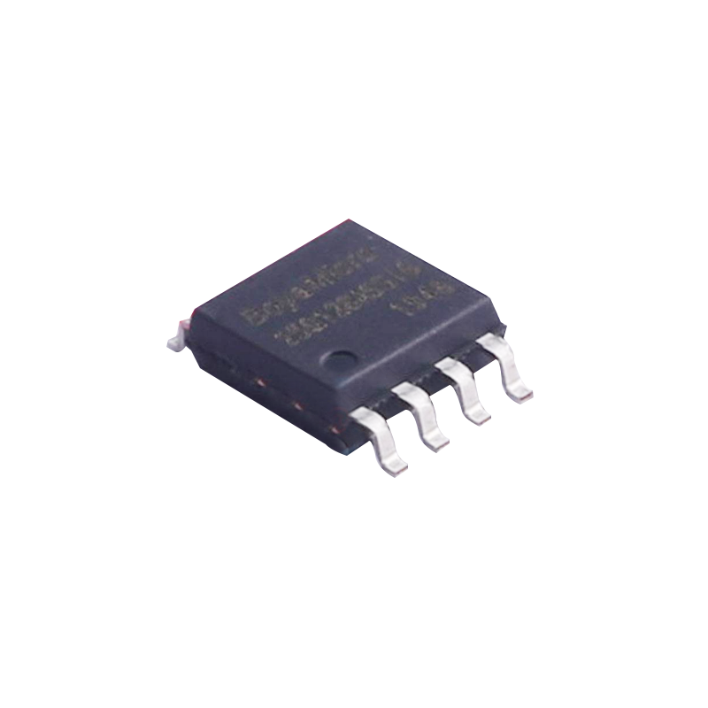
BY25Q16BSTIG 16M BIT SPI NOR FLASH electronic component wholesalers
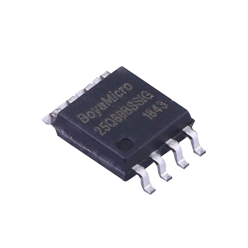
Boyamicro BY25Q80BSTIG FLASH NOR (SLC) Memory IC 8Mbit SPI – Quad I/O, QPI 108 MHz 7 ns 8-SOP electronic component supplier
The BY25Q16BSTIG is 16M-bit Serial Peripheral Interface(SPI) Flash memory, and supports the Dual/Quad SPI as well as 2-clocks instruction cycle Quad Peripheral Interface (QPI): Serial Clock, Chip Select, Serial Data I/O0 (SI), I/O1 (SO), I/O2 (/WP), and I/O3 (/HOLD). The Dual I/O data is transferred with speed of 216Mbits/s and the Quad I/O & Quad output data is transferred with speed of 432Mbits/s. The device uses a single low voltage power supply, ranging from 2.7 Volt to 3.6 Volt.
Additionally, the device supports JEDEC standard manufacturer and device ID and three 256-bytes Security Registers.
In order to meet environmental requirements, Boya Microelectronics offers 8-pin SOP 208mil, 8-pad WSON 6×5-mm, and other special order packages, please contacts Boya Microelectronics for ordering information.
Serial Peripheral Interface
– Standard SPI: SCLK, /CS, SI, SO, /WP, /HOLD
– Dual SPI: SCLK, /CS, IO0, IO1, /WP, /HOLD
– Quad SPI: SCLK, /CS, IO0, IO1, IO2, IO3
– QPI: SCLK, /CS, IO0, IO1, IO2, IO3
Read
– Normal Read (Serial): 55MHz clock rate
– Fast Read (Serial): 108MHz clock rate with 30PF load
– Dual I/O data transfer up to 216Mbits/S
– Quad I/O data transfer up to 432Mbits/S
– Allows XIP (execute in place) Operation: Continuous Read with 8/16/32/64-byte Wrap
Program
– Serial-input Page Program up to 256bytes
– Program Suspend and Resume
Erase
– Block erase (64/32 KB)
– Sector erase (4 KB)
– Chip erase
– Erase Suspend and Resume
Program/Erase Speed
– Page Program time: 0.6ms typical
– Sector Erase time: 50ms typical
– Block Erase time: 0.15/0.25s typical
– Chip Erase time: 15s typical
Flexible Architecture
– Sector of 4K-byte
– Block of 32/64K-byte
Low Power Consumption
– 20mA maximum active current
– 5uA maximum power down current
Software/Hardware Write Protection
– 3×256-Byte Security Registers with OTP Locks
– Discoverable Parameters (SFDP) register
– Enable/Disable protection with WP Pin
– Write protect all/portion of memory via software
– Top or Bottom, Sector or Block selection
Single Supply Voltage
– Full voltage range: 2.7~3.6V
Temperature Range
– Commercial (0℃ to +70℃)
– Industrial (-40℃ to +85℃)
– Industrial (-40℃ to +105℃)
Cycling Endurance/Data Retention
– Typical 100k Program-Erase cycles on any sector
– Typical 20-year data retention
| Type | BY25Q16BSTIG |
| Category | Memory |
| Packaging | Tube |
| Product Status | Active |
| Memory Type | Non-Volatile |
| Memory Format | FLASH |
| Technology | FLASH – NOR (SLC) |
| Memory Size | 16Mbit |
| Memory Organization | 2M x 8 |
| Memory Interface | SPI – Dual I/O,QPI |
| Clock Frequency | 108 MHz |
| Write Cycle Time – Word, Page | 50µs,2.4ms |
| Access Time | 7 ns |
| Voltage – Supply | 2.7V ~ 3.6V |
| Operating Temperature | -40°C ~ 85°C |
| Mounting Type | Surface Mount |
| Package / Case | 8-SOIC (0.154″, 3.90mm Width) |
| Supplier Device Package | 8-SOP |


