- Sorry, this product cannot be purchased.
Product Details
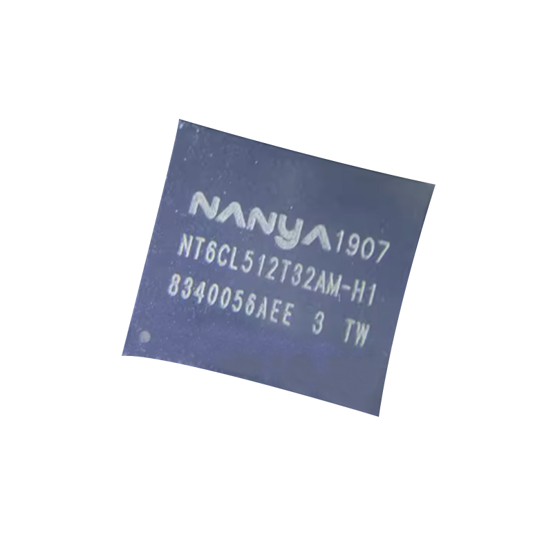
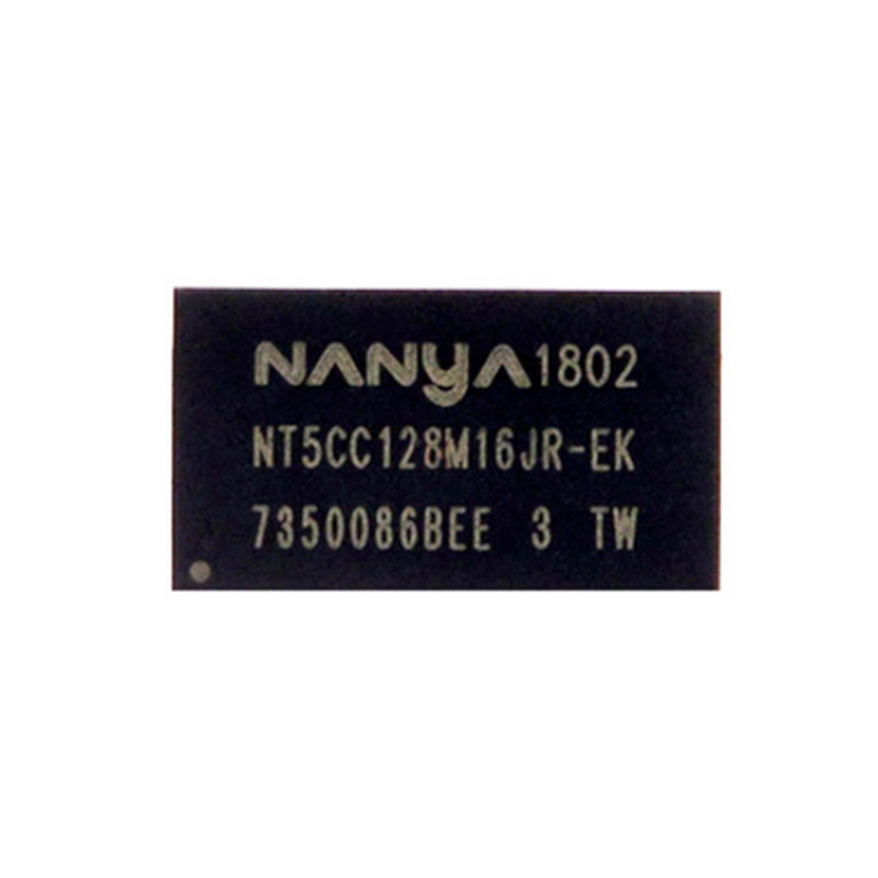
NT5CC256M16EP-EK DDR3L 4Gb SDRAM Commercial electronic component supplier
Electronic component wholesalers DDR3L 4Gb SDRAM Commercial Nanya NT5CC256M16EP-EK
Basis DDR3 Compliant
– 8n Prefetch Architecture
– Differential Clock(CK/CK) and Data Strobe(DQS/DQS)
– Double-data rate on DQs, DQS and DM
Data Integrity
– Auto Self Refresh (ASR) by DRAM built-in TS
– Auto Refresh and Self Refresh Modes
Power Saving Mode
– Power Down Mode
Signal Integrity
– Configurable DS for system compatibility
– Configurable On-Die Termination
– ZQ Calibration for DS/ODT impedance accuracy via
external ZQ pad (240 ohm ± 1%)
Signal Synchronization
– Write Leveling via MR settings 5
– Read Leveling via MPR
Interface and Power Supply
– SSTL_15 for DDR3:VDD/VDDQ=1.5V(±0.075V)
– SSTL_1352 for DDR3L:VDD/VDDQ=1.35V(-0.067/+0.1V)
Options
Speed Grade (CL-TRCD-TRP) 1
– 2133 Mbps / 14-14-14
– 1866 Mbps / 13-13-13
– 1600 Mbps / 11-11-11
Temperature Range (Tc) 3
– Commercial Grade = 0℃~95℃
– Quasi Industrial Grade (-T) = -40℃~95℃
– Industrial Grade (-I) = -40℃~95℃
Programmable Functions
CAS Latency (6/7/8/9/10/11/13/14)
CAS Write Latency (5/6/7/8/9/10)
Additive Latency (0/CL-1/CL-2)
Write Recovery Time (5/6/7/8/10/12/14/16)
Burst Type (Sequential/Interleaved)
Burst Length (BL8/BC4/BC4 or 8 on the fly)
Self RefreshTemperature Range(Normal/Extended)
Output Driver Impedance (34/40)
On-Die Termination of Rtt_Nom(20/30/40/60/120)
On-Die Termination of Rtt_WR(60/120)
Precharge Power Down (slow/fast)
The DDR3(L) SDRAM is a high-speed dynamic random access memory internally configured as an eight-bank DRAM.
The DDR3(L) SDRAM uses an 8n prefetch architecture to achieve high speed operation. The 8n prefetch architecture is combined with an interface designed to transfer two data words per clock cycle at the I/O pins. A single read or write operation for the DDR3(L) SDRAM consists of a single 8n-bit wide, four clock data transfer at the internal DRAM core and eight corresponding n-bit wide, one-half clock cycle data transfers at the I/O pins.
Read and write operation to the DDR3(L) SDRAM are burst oriented, start at a selected location, and continue for a burst length of eight or a ‘chopped’ burst of four in a programmed sequence. Operation begins with the registration of an Active command, which is then followed by a Read or Write command. The address bits registered coincident with the Active command are used to select the bank and row to be activated (BA0-BA2 select the bank; A0-A15 select the row). The
address bit registered coincident with the Read or Write command are used to select the starting column location for the burst operation, determine if the auto precharge command is to be issued (via A10), and select BC4 or BL8 mode’on the fly'(via A12) if enabled in the mode register.
Prior to normal operation, the DDR3(L) SDRAM must be powered up and initialized in a predefined manner. The following sections provide detailed information covering device reset and initialization, register definition, command descriptions and device operation.
Organization: 256M x 16
Part Number : NT5CC256M16EP-EK
Package: 96-Ball
Speed Clock (MHz): 933
Speed Data Rate (Mb/s) : DDR3L-1866
Speed CL-TRCD-TRP: 13-13-13
| Model | NT5CC256M16EP-EK |
| DRAM Density | 4Gb |
| Config | x16 |
| Voltage | 1.35V |
| Package | 96-ball BGA |
| Speed | 1866Mbps |
| Temperature | 0C~95C |
| Grade | Commercial |


